Magnetization Manipulation of a Flexible Magnetic Sensor by Controlled Stress Application
- PMID: 30361479
- PMCID: PMC6202418
- DOI: 10.1038/s41598-018-34036-z
Magnetization Manipulation of a Flexible Magnetic Sensor by Controlled Stress Application
Erratum in
-
Publisher Correction: Magnetization Manipulation of a Flexible Magnetic Sensor by Controlled Stress Application.Sci Rep. 2018 Nov 29;8(1):17579. doi: 10.1038/s41598-018-36017-8. Sci Rep. 2018. PMID: 30498226 Free PMC article.
Abstract
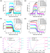
Spin-based electronic devices on polymer substrates have been intensively investigated because of several advantages in terms of weight, thickness, and flexibility, compared to rigid substrates. So far, most studies have focused on maintaining the functionality of devices with minimum degradation against mechanical deformation, as induced by stretching and bending of flexible devices. Here, we applied repetitive bending stress on a flexible magnetic layer and a spin-valve structure composed of Ta/NiFe/CoFe/Cu/Ni/IrMn/Ta on a polyimide (PI) substrate. It is found that the anisotropy can be enhanced or weakened depending upon the magnetostrictive properties under stress. In the flat state after bending, due to residual compressive stress, the magnetic anisotropy of the positive magnetostrictive free layer is weakened while that of the pinned layer with negative magnetostriction is enhanced. Thus, the magnetic configuration of the spin-valve is appropriate for use as a sensor. Through the bending process, we design a prototype magnetic sensor cell array and successfully show a sensing capability by detecting magnetic microbeads. This attempt demonstrates that appropriate control of stress, induced by repetitive bending of flexible magnetic layers, can be effectively used to modify the magnetic configurations for the magnetic sensor.
Conflict of interest statement
The authors declare no competing interests.
Figures


Similar articles
-
Mechanical Strain Manipulation of Exchange Bias Field and Spin Dynamics in FeCo/IrMn Multilayers Grown on Flexible Substrates.ACS Appl Mater Interfaces. 2019 Feb 27;11(8):8258-8265. doi: 10.1021/acsami.8b21421. Epub 2019 Feb 12. ACS Appl Mater Interfaces. 2019. PMID: 30697995
-
Electric Field-Tunable Giant Magnetoresistance (GMR) Sensor with Enhanced Linear Range.ACS Appl Mater Interfaces. 2020 Feb 19;12(7):8855-8861. doi: 10.1021/acsami.9b20038. Epub 2020 Feb 6. ACS Appl Mater Interfaces. 2020. PMID: 31984722
-
Greatly Improved the Tunable Amplitude of Ferromagnetism Based on Interface Effect of Flexible Pt/YIG Heterojunctions.ACS Appl Mater Interfaces. 2024 Feb 28;16(8):10953-10959. doi: 10.1021/acsami.3c17220. Epub 2024 Feb 13. ACS Appl Mater Interfaces. 2024. PMID: 38350012
-
Thin-Film Heterostructures Based on Co/Ni Synthetic Antiferromagnets on Polymer Tapes: Toward Sustainable Flexible Spintronics.ACS Appl Mater Interfaces. 2022 Nov 16;14(45):51496-51509. doi: 10.1021/acsami.2c14000. Epub 2022 Nov 1. ACS Appl Mater Interfaces. 2022. PMID: 36318544
-
Review of the Development of an Unbonded Flexible Riser: New Material, Types of Layers, and Cross-Sectional Mechanical Properties.Materials (Basel). 2024 May 26;17(11):2560. doi: 10.3390/ma17112560. Materials (Basel). 2024. PMID: 38893824 Free PMC article. Review.
Cited by
-
Adjusting microwave sensing frequency through aspect ratio variation and bending repetitions in Permalloy ellipses.Sci Rep. 2024 Jul 24;14(1):17070. doi: 10.1038/s41598-024-66802-7. Sci Rep. 2024. PMID: 39048623 Free PMC article.
-
Flexible Magnetic Sensors.Sensors (Basel). 2023 Apr 18;23(8):4083. doi: 10.3390/s23084083. Sensors (Basel). 2023. PMID: 37112422 Free PMC article. Review.
-
Two-dimensional arrays of vertically packed spin-valves with picoTesla sensitivity at room temperature.Sci Rep. 2021 Jan 8;11(1):215. doi: 10.1038/s41598-020-79856-0. Sci Rep. 2021. PMID: 33420189 Free PMC article.
-
Spiral Annealing of Magnetic Microwires.Sensors (Basel). 2024 Sep 26;24(19):6239. doi: 10.3390/s24196239. Sensors (Basel). 2024. PMID: 39409279 Free PMC article.
-
Giant Magnetoimpedance Effect of Multilayered Thin Film Meanders Formed on Flexible Substrates.Micromachines (Basel). 2023 May 6;14(5):1002. doi: 10.3390/mi14051002. Micromachines (Basel). 2023. PMID: 37241625 Free PMC article.
References
-
- Zhou L, et al. All-organic active matrix flexible display. Appl. Phys. Lett. 2006;88:083502. doi: 10.1063/1.2178213. - DOI
-
- Krebs FC, Gevorgyan SA, Alstrup J. A roll-to-roll process to flexible polymer solar cells: model studies, manufacture and operational stability studies. J. Mater. Chem. 2009;19:5442–5451. doi: 10.1039/b823001c. - DOI
Grants and funding
LinkOut - more resources
Full Text Sources
Other Literature Sources
Research Materials
Miscellaneous

