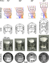
3D-printed eagle eye: Compound microlens system for foveated imaging
- PMID: 28246646
- PMCID: PMC5310822
- DOI: 10.1126/sciadv.1602655
3D-printed eagle eye: Compound microlens system for foveated imaging
Abstract
We present a highly miniaturized camera, mimicking the natural vision of predators, by 3D-printing different multilens objectives directly onto a complementary metal-oxide semiconductor (CMOS) image sensor. Our system combines four printed doublet lenses with different focal lengths (equivalent to f = 31 to 123 mm for a 35-mm film) in a 2 × 2 arrangement to achieve a full field of view of 70° with an increasing angular resolution of up to 2 cycles/deg field of view in the center of the image. The footprint of the optics on the chip is below 300 μm × 300 μm, whereas their height is <200 μm. Because the four lenses are printed in one single step without the necessity for any further assembling or alignment, this approach allows for fast design iterations and can lead to a plethora of different miniaturized multiaperture imaging systems with applications in fields such as endoscopy, optical metrology, optical sensing, surveillance drones, or security.
Keywords: 3D printing; foveated imaging; micro camera; multi-aperture imaging systems.
Figures


Similar articles
-
Distortion-free multi-element Hypergon wide-angle micro-objective obtained by femtosecond 3D printing.Opt Lett. 2020 May 15;45(10):2784-2787. doi: 10.1364/OL.392253. Opt Lett. 2020. PMID: 32412466
-
Micro-optical artificial compound eyes.Bioinspir Biomim. 2006 Mar;1(1):R1-16. doi: 10.1088/1748-3182/1/1/R01. Epub 2006 Apr 6. Bioinspir Biomim. 2006. PMID: 17671298 Review.
-
Design and fabrication of a freeform microlens array for a compact large-field-of-view compound-eye camera.Appl Opt. 2012 Apr 20;51(12):1843-52. doi: 10.1364/AO.51.001843. Appl Opt. 2012. PMID: 22534888
-
Miniaturized 3D Depth Sensing-Based Smartphone Light Field Camera.Sensors (Basel). 2020 Apr 9;20(7):2129. doi: 10.3390/s20072129. Sensors (Basel). 2020. PMID: 32283826 Free PMC article.
-
Artificial Compound Eye Systems and Their Application: A Review.Micromachines (Basel). 2021 Jul 20;12(7):847. doi: 10.3390/mi12070847. Micromachines (Basel). 2021. PMID: 34357257 Free PMC article. Review.
Cited by
-
Mid-infrared polarization-controlled broadband achromatic metadevice.Sci Adv. 2020 Sep 11;6(37):eabc0711. doi: 10.1126/sciadv.abc0711. Print 2020 Sep. Sci Adv. 2020. PMID: 32917714 Free PMC article.
-
3D printed fiber optic faceplates by custom controlled fused deposition modeling.Opt Express. 2018 Jun 11;26(12):15362-15376. doi: 10.1364/OE.26.015362. Opt Express. 2018. PMID: 30114785 Free PMC article.
-
A Meniscus Multifocusing Compound Eye Camera Based on Negative Pressure Forming Technology.Micromachines (Basel). 2023 Feb 10;14(2):420. doi: 10.3390/mi14020420. Micromachines (Basel). 2023. PMID: 36838120 Free PMC article.
-
Biologically inspired ultrathin arrayed camera for high-contrast and high-resolution imaging.Light Sci Appl. 2020 Feb 27;9:28. doi: 10.1038/s41377-020-0261-8. eCollection 2020. Light Sci Appl. 2020. PMID: 32140219 Free PMC article.
-
Miniature optoelectronic compound eye camera.Nat Commun. 2022 Sep 26;13(1):5634. doi: 10.1038/s41467-022-33072-8. Nat Commun. 2022. PMID: 36163128 Free PMC article.
References
-
- Guo R., Xiao S., Zhai X., Li J., Xia A., Huang W., Micro lens fabrication by means of femtosecond two photon photopolymerization. Opt. Express 14, 810.– (2006). - PubMed
-
- Winfield R., Bhuian B., O’Brien S. C. G., Crean G. M., Fabrication of grating structures by simultaneous multi-spot fs laser writing. Appl. Surf. Sci. 253, 8086.– (2007).
-
- Lindenmann N., Balthasar G., Hillerkuss D., Schmogrow R., Jordan M., Leuthold J., Freude W., Koos C., Photonic wire bonding: A novel concept for chip-scale interconnects. Opt. Express 20, 17667–17677 (2012). - PubMed
-
- Thiele S., Gissibl T., Giessen H., Herkommer A. M., Ultra-compact on-chip LED collimation optics by 3D femtosecond direct laser writing. Opt. Lett. 41, 3029–3032 (2016). - PubMed
-
- Liberale C., Cojoc G., Candeloro P., Das G., Gentile F., De Angelis F., Di Fabrizio E., Micro-optics fabrication on top of optical fibers using two-photon lithography. IEEE Photonics Technol. Lett. 22, 474–476 (2010).
LinkOut - more resources
Full Text Sources
Other Literature Sources

